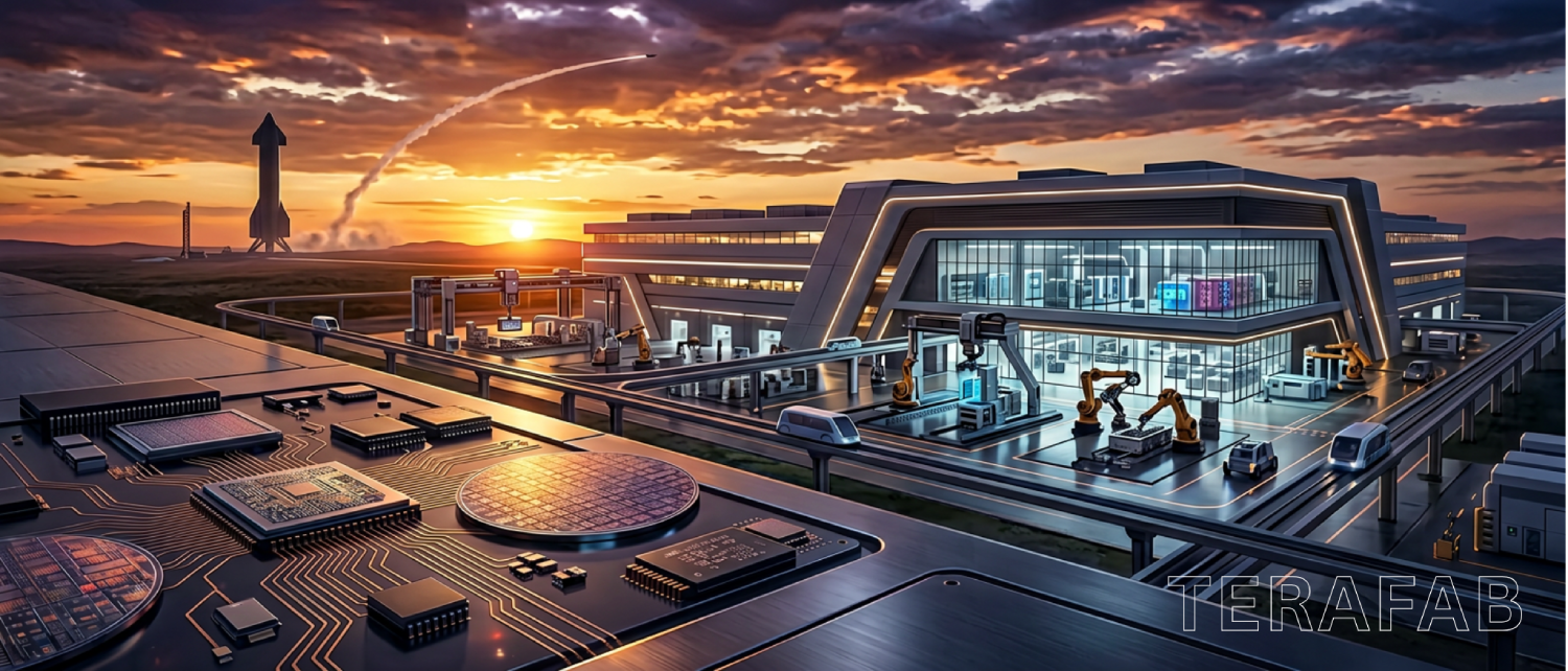
Terafab is a planned vertically integrated semiconductor fabrication complex, jointly developed by Tesla, SpaceX, and xAI, officially announced by Elon Musk on March 21, 2026, at the historic Seaholm Power Plant in Austin, Texas. With an estimated budget of $20–25 billion, it targets a production capacity of one terawatt (one trillion watts) of AI computing power per year, roughly 50 times the estimated output of all the world’s current advanced AI chip manufacturers combined. Musk called it “the most epic chip-building exercise in history by far” and framed it as a necessary step toward humanity becoming a multi-planetary, even “galactic civilization”.
The project aims to consolidate every stage of chip production, design, lithography, fabrication, memory, advanced packaging, and testing under one roof, a level of vertical integration never before attempted at this scale. Its first products will be the AI5 inference chip for Tesla autonomous vehicles and Optimus robots, and the D3 space-hardened chip for SpaceX orbital AI satellites.
Terafab did not emerge from ambition alone. It was a direct response to a supply chain crisis that Musk had been signaling publicly since 2024. The core problem: exponential demand from Tesla Full Self-Driving (FSD), Cybercab robotaxi program, and Optimus humanoid robot project was on a collision course with global foundry capacity limits.
At the Tesla Q4 2025 earnings call on January 28, 2026, Musk confirmed the urgency: external chip capacity from suppliers like TSMC, Samsung, and Micron would hit a ceiling within three to four years. He stated plainly: “We’re very grateful to our existing supply chain, to Samsung, TSMC, Micron and others, but there’s a maximum rate at which they’re comfortable expanding.
The numbers reveal the scale of the gap. Musk claimed that all fabrication facilities on Earth collectively produce approximately 20 gigawatts of AI compute annually, roughly 2% of what his companies would need at full scale. A single Morgan Stanley analyst noted that Tesla’s Giga Texas alone is projected to require capacity for 10 million Optimus robots per year, demanding around 20 million chips, about six times Tesla’s entire current automotive chip demand. At the stated long-term goal of 100 million Optimus robots, demand would exceed 200 million chips, more than 50 times Tesla’s current output across automotive and robotaxi sectors.
The conclusion Musk drew was characteristically blunt: “We either build the Terafab, or we don’t have the chips, and we need the chips, so we’re going to build the Terafab.”
On March 14, 2026, Musk posted on X (formerly Twitter): “Terafab Project launches in 7 days”, ending a period of speculation that had built for over a year. The official unveiling took place at the defunct Seaholm Power Plant in Austin on March 21, 2026, a symbolically chosen venue, with the event livestreamed on SpaceX’s broadcast channel. Musk used the occasion not just to describe a chip factory, but to lay out a sweeping vision for civilization itself.
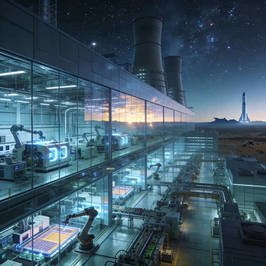
Terafab is not a conventional semiconductor foundry. It is best understood as a fully integrated chip ecosystem, a single facility combining every element of semiconductor production that is normally distributed across dozens of specialized vendors around the world. The planned location is the North Campus of Giga Texas in eastern Travis County, Austin, a site expected to surpass the footprint of Giga Texas itself, already one of the largest buildings on Earth.
The facility is technically structured as two dedicated fabs, each focused on one chip architecture:
The full-scale Terafab will be built at a yet-to-be-determined location, with the Austin site serving as the initial prototype and pilot production facility.
Technical Specifications
| Specification | Detail |
| Estimated Investment | $20–25 billion |
| Process Node | 2-nanometer (2nm), most advanced in commercial production |
| Initial Output | 100,000 wafer starts per month |
| Full-Scale Target | 1,000,000 wafer starts per month (~70% of TSMC current global output) |
| Annual Chip Output | 100–200 billion custom AI and memory chips |
| Compute Capacity | 1 terawatt (1 trillion watts) per year |
| Official Announcement | March 21, 2026 |
| Pilot Small-Batch Production | Late 2026 (AI5) |
| Volume Production Start | 2027 (projected) |
Terafab targets 2-nanometer process technology, using Extreme Ultraviolet (EUV) lithography, the same cutting-edge node that TSMC is only beginning to deploy at scale, having spent decades and hundreds of billions of dollars reaching this capability. The facility will co-locate on-package High-Bandwidth Memory (HBM) directly with logic dies to reduce data movement bottlenecks critical for AI inference workloads.
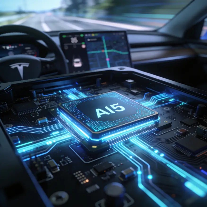
Tesla AI5 chip is Terafab’s first product and the crown jewel of the terrestrial side. Compared to the current AI4 system, the AI5 delivers approximately 40–50x more compute performance and 9x more memory bandwidth. Designed for edge inference, meaning real-time, on-device computation rather than cloud-based training, the AI5 will process an estimated 10–20 trillion operations per second to support Tesla Full Self-Driving system in split-second driving decisions. Small-batch production of AI5 is anticipated in late 2026, with volume production in 2027.
The AI6 chip will follow for even more demanding workloads, particularly those required by Optimus humanoid robots performing complex physical tasks at scale. Tesla’s existing supply agreements remain in place during ramp-up: AI5 is currently manufactured by TSMC (initially in Taiwan, transitioning to Arizona), and AI6 is under a $16.5 billion contract with Samsung’s Taylor, Texas fab through 2033. Terafab, if built, becomes a third leg of the supply chain rather than an immediate replacement.
The Space Chip
The D3 chip is arguably the more ambitious product. It is a high-power, radiation-hardened processor specifically designed to operate in the vacuum and extreme temperature swings of low Earth orbit (LEO). No consumer-grade chip can meet the specifications required by the orbital environment, including resistance to cosmic radiation and the absence of conventional cooling, making D3 a purpose-built, unprecedented product.
Musk stated that approximately 80% of Terafab total compute output will be directed toward space applications, with only 20% going to terrestrial use. That allocation, four-fifths of the world’s most ambitious chip factory pointed at space, is one of the most revealing indicators of Terafab’s true strategic purpose.
The Terafab vision extends far beyond chip manufacturing. Central to Musk announcement was the concept of moving AI compute infrastructure off Earth and into orbit. The rationale rests on three physical advantages of space over terrestrial data centers:
Musk debuted a concept design for a “Mini AI Satellite”, a small orbital compute node delivering 100 kilowatts of power from an exceptionally long solar array, with future units projected to reach the megawatt range. SpaceX has already filed with the Federal Communications Commission (FCC) to deploy up to one million data center satellites in orbit, potentially creating the world’s largest distributed computing network in space.
Musk framed Terafab not as a business project but as a civilizational one. He referenced the Kardashev Scale, the theoretical framework for measuring a civilization’s energy consumption, explicitly describing the goal as advancing humanity toward Type II or higher civilization status, capable of harnessing stellar-scale energy.
“We aspire to be a galactic civilization… the future that most people would agree is the most exciting is one where we are out there among the stars, where we are not forever confined to one planet,” Musk said at the event.
In his most expansive statements, Musk described a future where electromagnetic mass drivers on the Moon launch AI compute infrastructure into deep space, eventually reaching a petawatt of computing power beyond Earth. These scales would make current global computing look trivial.
The practical near-term case centers on a simpler argument: training runs and batch AI workloads that take days to complete have no latency requirement, making them strong candidates for orbital migration once launch costs fall to a sufficient threshold. Musk projected that within two to three years, running certain AI workloads in orbit would become cheaper than doing so on Earth.
Terafab represents the most ambitious attempt at semiconductor vertical integration in commercial history. TSMC operates as a contract foundry for hundreds of customers; Terafab will produce only two proprietary chip designs, solely for Tesla, SpaceX, and xAI. This hyper-focused model allows optimization of every manufacturing step for a known workload, a different philosophy from general-purpose foundry economics.
The venture unites three of Musk’s major companies in a single supply chain: Tesla (AI5/AI6 chips for cars and robots), SpaceX/xAI (D3 chips for orbital satellites and data centers), with xAI having been formally acquired by SpaceX in an all-stock deal in February 2026. The combination places Musk in control of the hardware, the software, the robotics, the rockets, and now the chip foundry, a degree of vertical integration with no precedent in the technology industry.
Terafab’s narrative reinforces broader US policy goals around reducing reliance on Taiwanese semiconductor production. As AI has become a defining national security technology, the concentration of advanced chip manufacturing in Taiwan and the associated risks of geopolitical disruption have made domestic semiconductor capacity a strategic priority for Washington. Terafab positions Texas as a potential hub for advanced semiconductor manufacturing, complementing TSMC own Arizona expansion.
Within days of the announcement, Tesla began aggressively recruiting semiconductor engineers in Taiwan and South Korea, explicitly targeting TSMC and Samsung Foundry employees. Tesla posted job listings in Taiwan seeking engineers with over 10 years of experience, specifying expertise in Gate-All-Around (GAA) and FinFET processes, as well as backside power delivery network (BSPDN) technology, the most critical roles in leading-edge foundry operations. Musk posted on X: “If you live in Korea and want to work in chip design, fab, or AI software, apply to Tesla.” Industry observers in Taiwan have raised concerns about potential talent outflows from TSMC as Tesla’s aggressive push accelerates.
The announcement met significant skepticism from semiconductor industry analysts and executives. NVIDIA CEO Jensen Huang, whose company relies on TSMC for manufacturing, publicly warned in November 2025: “Building advanced chip manufacturing is extremely hard. It is not just building the plant, but the engineering, the science, and the artistry of doing what TSMC does for a living is extremely hard.” Huang went further, calling matching TSMC capabilities “virtually impossible.”
Stacy Rasgon, a senior semiconductor analyst at Bernstein, told Business Insider: “It’s Musk, so I would never count it out. But I suspect this is actually harder than sending rockets to Mars.” Rasgon’s firm estimated that achieving Terafab stated 1-terawatt output goal would require the equivalent of 142 to 358 new leading-edge fabs, implying capital expenditure of $5 trillion to $13 trillion, comparable to or exceeding the entire current global semiconductor manufacturing base.
Bank of America Securities estimated that bringing Terafab to operational readiness would take at least three to five years of construction and qualification, pushing mass production to 2029 at the earliest, not 2027 as Musk implied. BofA also estimated that an initial 100,000-wafer-per-month capacity alone could require more than $60 billion in capital expenditure, far above the stated $20–25 billion project budget. Even at full utilization, wafer costs at Terafab are expected to be 30–50% higher than TSMC advanced nodes, due to a lack of scale economies and an immature process ecosystem.
Critics have drawn explicit comparisons to Tesla’s Battery Day in 2020, when Musk made sweeping promises about the 4680 battery cell that took years longer than promised to deliver and fell significantly short of initial targets. Tesla’s own Dojo supercomputer project was canceled, revived, renamed, and partially absorbed into the AI6 program, all within six months of its most recent announcement. As of the Terafab launch, the AI5 chip had been described as “finished” in July 2025, “almost done” in January 2026, and was reportedly still not taped out in March 2026.
TSMC, by comparison, spent decades and hundreds of billions of dollars building its manufacturing expertise. Intel, which has thousands of experienced fab engineers and over $100 billion in investments, has struggled for years to regain its manufacturing edge at advanced nodes. Samsung foundry business, despite massive investment, still trails TSMC in yield rates.
Not all observers dismiss the project. Musk track record includes genuinely unprecedented achievements: reusable orbital rockets (Falcon 9), gigafactory-scale battery cell production, and the world’s first mass-market autonomous vehicle fleet. Analysts note that Tesla has already demonstrated significant in-house chip design capability, AI4 is a competitive processor, and that the Terafab venture, even if it achieves only partial goals, would meaningfully de-risk Tesla’s chip supply and accelerate iteration cycles on proprietary hardware.
Tom’s Hardware’s analysis acknowledged that even a partial realization, a pilot fab producing AI5 in limited quantities, would constitute a historic milestone: a consumer technology company building its own leading-edge semiconductor manufacturing from scratch.
| Entity | Model | Process Node | Annual Output | Capital Investment |
| TSMC (global) | Contract foundry | 2nm (deploying) | ~1.4M wafer starts/month | $165B (Arizona alone) |
| Samsung Foundry | Contract foundry | 3nm | ~600K wafer starts/month | $17B (Taylor, TX) |
| Intel Foundry | IDM + contract | 18A/2nm (developing) | Limited at advanced nodes | $100B+ cumulative |
| Terafab (target) | Captive vertical | 2nm | 100K → 1M starts/month | $20–25B stated |
Terafab full-scale one-million-wafer-per-month ambition would represent approximately 70% of TSMC’s current total global output, from a single facility operated by a company that has never fabricated a wafer. In the near term, analysts at BofA and Bernstein agree that Terafab poses limited disruption risk to TSMC due to execution timelines, cost disadvantages, and the lack of a supporting ecosystem.
| Date | Event |
| 2024 Tesla AGM | Musk first warns of long-term chip supply insufficiency |
| January 28, 2026 | Q4 2025 earnings call, Terafab officially confirmed; supply crisis projected within 3–4 years |
| February 2026 | SpaceX acquires xAI in all-stock deal |
| March 14, 2026 | Musk posts on X: “Terafab Project launches in 7 days.” |
| March 21, 2026 | Official Terafab announcement at Seaholm Power Plant, Austin |
| March 23–24, 2026 | Tesla begins recruiting semiconductor engineers in Taiwan and South Korea |
| Late 2026 | Small-batch AI5 production anticipated at pilot fab |
| 2027 | Volume AI5 production projected |
| 2029+ | BofA estimate for the earliest realistic mass production at scale |
Terafab’s most immediate near-term impact is in semiconductor equipment demand. Bernstein’s Rasgon noted that even if pursued at a fraction of its stated scale, the buildout would represent a major demand driver for chipmaking equipment makers, implying investors should watch semiconductor capital equipment companies closely. The aggressive talent acquisition campaign in Taiwan and Korea is already creating ripple effects in the global semiconductor workforce market.
For the broader AI industry, Terafab signals that the compute bottleneck, not algorithms or data, is increasingly seen as the binding constraint on AI progress. Musk’s estimate that current global AI chip production meets only about 2% of his company projected needs reflects a demand trajectory that, if accurate, would require restructuring the entire global semiconductor industry.
For the US policy environment, Terafab amplifies the argument for domestic semiconductor investment. Alongside TSMC Arizona and Intel’s Ohio fab projects, Terafab would, if completed, make the United States a more credible counterweight to Taiwan’s current dominance in advanced chip manufacturing.
Terafab is simultaneously the most ambitious semiconductor project in history and one of the most contested. Elon Musk launched it not because it was easy, but because his company projected demand for AI compute made dependence on external foundries an existential supply chain risk. The vision, chips for Earth, chips for space, and a pathway to a galactic civilization, is uniquely Musk, expansive, urgent, and technically controversial.
Whether Terafab delivers on its 1-terawatt promise by 2027, or whether it takes a decade and three times the stated budget, its launch marks a structural shift in how the most compute-hungry companies on Earth are beginning to think about silicon. The question is no longer whether AI needs more chips; it does, at a scale the current industry cannot match. The question is who builds them, and whether Terafab can compress decades of semiconductor learning into a few years of audacious engineering.
Hassan Tahir wrote this article, drawing on his experience to clarify WordPress concepts and enhance developer understanding. Through his work, he aims to help both beginners and professionals refine their skills and tackle WordPress projects with greater confidence.


 Lifetime Hosting
 France Lifetime Dedicated Servers
 Germany Lifetime dedicated servers
 Lifetime Game Dedicated Servers
 Chicago, US
 Singapore
 Hong Kong
 Seoul, South Korea
 Amsterdem, Netherlands
 London, UK
 Zurich, Switzerland
 Sydney, Australia
 DDOS Protection
 Submit Ticket
 Full Management
 Videos and Podcasts
 Voxfor Advanced Price Management For WooCommerce
 Voxfor AI Content Summary


