
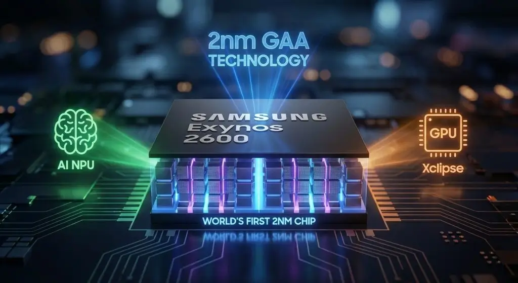
The Exynos 2600 is the first smartphone system-on-chip (SoC) in the world to be produced with Gate-All-Around (GAA) process technology with a 2-nanometer Gate. The declaration marks a break-even point in the history of Samsung mobile chip business, as years have been wasted in second place to Snapdragon-based offerings of Qualcomm. With mass production already in the pipeline, Exynos 2600 can be used to drive the Galaxy S26 and Galaxy S26+ series that will launch at the beginning of 2026 and can become a potential inflection point in the competitiveness of Samsung in the high-end smartphone markets.
The Exynos 2600 embodies Samsung’s bet that architectural innovations and manufacturing leadership can overcome the chip design challenges that have historically plagued its flagship processors.The 2nm GAA process achieves 12% performance and 25 percent efficiency, and reportedly achieved more than 50 percent yields, a crucial stage in the process maturity and scalability.
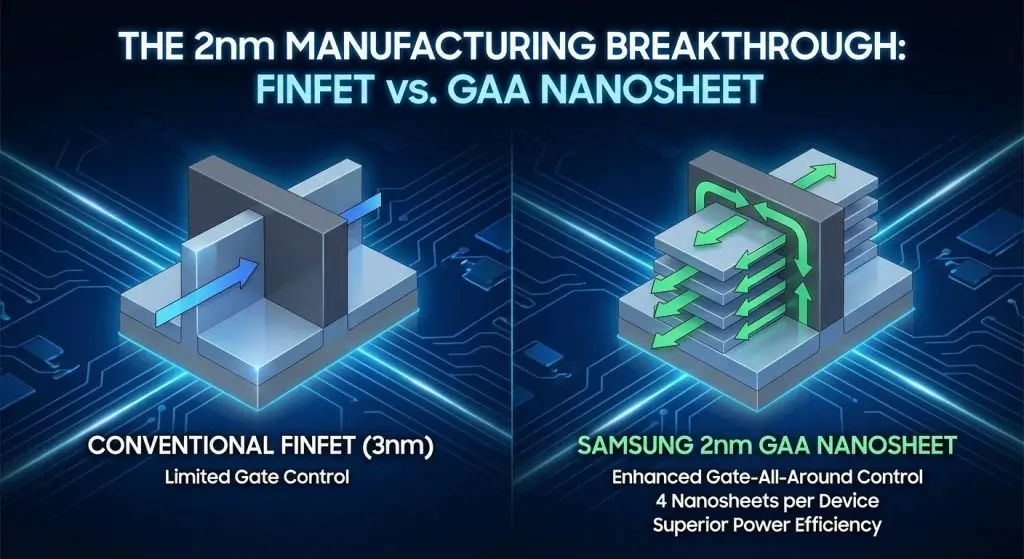
It would be important to figure out what makes the Samsung 2nm GAA process truly transformative in order to understand the importance of the Exynos 2600. Gate-All-Around transistor technology is a nanosheet FET design that allows a higher current flow rate and better power efficiency in comparison with other FinFET designs.
The technical advantage is substantial. Samsung 2nm uses nanosheet transistors, with four nanosheets per device, an increase from three in the previous 3nm generation. This nanosheet structure enables the transistors to manage current flow on several sides to provide better performance density and finer-grain power control.
The ramifications are industry-influencing. In November 2025, Samsung started its mass production of 2nm, making it ahead of other competing foundries such as Intel and TSMC, which remain in their ramp production stages. The Intel 18A has an estimated yield of 50-55 percent, which possibly will not result in full-scale deliveries until 2026. TSMC 2nm schedule is still under delays and the production volume is not expected earlier than the end of 2026.
This timing advantage grants Samsung a critical window: the Exynos 2600 will be the first commercially available 2nm smartphone chip in mass production, setting the technological benchmark against which competitors will be measured throughout 2026.
The Exynos 2600 uses a 10-core CPU (with a 1-core physical layout) with an ARM v9.3 core architecture, disregarding the hybrid big-little implementation that has defined Samsung flagships in the past. The chip comes with one C1 Ultra core, three C1 Pro cores with 3.25GHz and six other cores with 2.75 GHz. This is a homogenous design as opposed to the asymmetric design of Qualcomm, but with the objective of achieving better sustained performance by offering better thermal performance.
Samsung claims 39% CPU performance improvement over the Exynos 2500. Independent Geekbench 6 benchmarks corroborate this claim: the Exynos 2600 achieves approximately 3,455 single-core and 11,621 multi-core points, representingroughly 37% improvement in single-core and 29% improvement in multi-core.
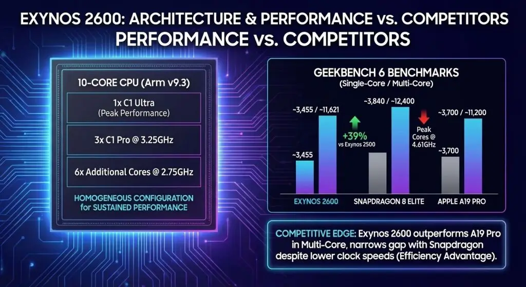
However, comparative analysis with competing flagship chips reveals nuanced performance dynamics.While the Exynos 2600 trails Snapdragon 8 Elite by approximately 10% single-core and 6.25% multi-core, this gap is remarkably narrow considering that Snapdragon peak cores operate at 4.61GHz versus Exynos’s 3.8GHz, approximately 21% higher clock frequency. This efficiency at lower clock speeds suggests architectural advantages in instruction-level parallelism or pipeline design.
Perhaps more significantly, early reports indicate Exynos 2600 outperforms Apple’s A19 Pro in multi-core Geekbench testing, making it competitive with or superior to the current generation of flagship mobile chips.
Beyond raw CPU performance, the Exynos 2600 represents a fundamental strategic shift toward on-device artificial intelligence capabilities. The chip includes a redesigned NPU claiming 113% improvement over the Exynos 2500, a dramatic leap that positions AI as a core competitive advantage.

Samsung claims Exynos 2600 NPU is approximately 30% ahead of Snapdragon 8 Elite Gen 5 in AI performance benchmarks, representing the most substantial single-metric advantage over competitors. The strategic consequences of this NPU performance advantage are as follows: AI processing loads on smartphone processors, whether in voice processing, computational photography or real-time translation, are progressively defining the quality of user experience and not the performance of the underlying CPU.
The design of this performance leap must be based on the experience that Samsung has gained in the past generations. Instead of positioning the NPU as an efficiency accelerator, it seems that Samsung has positioned it as a first-order compute engine for certain AI-intensive tasks.
The Exynos 2600 integrates the Xclipse 960 GPU, delivering double compute performance and 50% better ray-tracing over the previous Xclipse 950. Samsung introduced Exynos Neural Super Sampling (ENSS) technology, which leverages AI-based frame generation and upscaling to achieve smooth high-frame-rate gaming while minimizing power consumption.
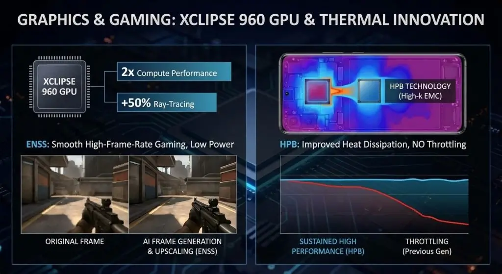
This GPU advancement addresses a persistent weakness in Exynos chips: thermal management under sustained gaming loads. Samsung developed Heat Path Block (HPB) technology using High-k EMC material to improve heat dissipation and deliver sustained high performance during extended gaming sessions. This heat management innovation directly addresses one of Samsung’s most damaging weaknesses, the “Exynos curse” of throttling under load, and may prove critical to real-world device performance.
The Exynos 2600 supports camera sensors up to 320 megapixels, extending the ISP (Image Signal Processor) capabilities beyond current flagship requirements. The chip integrates a new AI-based Visual Perception System, enabling more accurate scene and object recognition, and introducesdeep learning-based video noise reduction for improved low-light capture.
The emphasis on AI-assisted imaging reflects broader industry trends where computational photography, AI-powered processing rather than raw sensor capability, increasingly determines perceived image quality. Samsung investment in on-device AI processing for imaging acknowledges that users prioritize AI-assisted image enhancement over megapixel count.
The Exynos 2600 introduces hybrid post-quantum cryptography, a forward-looking security feature addressing the theoretical threat of quantum computing to current encryption standards.The chip incorporates virtualization security features, hardening against attacks that exploit virtual machine escape vulnerabilities.

This cryptographic strength is also indicative of how Samsung has been marketing the flagship mobile devices as safe havens to conduct sensitive activities, financial transactions, health information, and business-related communications. Hardware-supported post-quantum cryptography, although not yet the order of the day, indicates that Samsung has a future strategy of adopting future threats of cryptography to Galaxy S26 devices.
Samsung’s achievement exceeds 50% manufacturing yields, representing a crucial inflection point for 2nm production economics. Semiconductor manufacturing yields, the percentage of functional chips from a wafer, directly determine production costs and pricing flexibility. At 50%+ yields, Samsung can achieve cost structures comparable to mainstream 5nm production, enabling mainstream pricing rather than premium components.
The economic significance extends beyond Samsung.Samsung 2nm foundry will serve major customers, potentially capturing revenue from ARM-based and potentially other processor architectures seeking advanced manufacturing capability. Success in attracting foundry customers would fundamentally transform Samsung’s business model from device-centric to foundry-centric, similar to TSMC’s dominance.
Samsung’s deployment strategy for the Exynos 2600 remains partially unclear. Earlier reports suggested global deployment across Galaxy S26 and S26+ models, potentially including the Ultra variant, finally breaking a decade-long pattern of exclusive Snapdragon usage. However, more recent claims indicate limited regional deployment, possibly restricted to Korean and select Asian markets.
Such vagueness is an indication of internal Samsung calculations in the competitive positioning and supply chain optimization. This would be an indicator of confidence in the competitiveness of the chip; regional restriction would be an indicator of Samsung wanting to only supply the market in the optimal-cost range, or it may be an indication that it was unsure about the practical thermal performance of the chip at commercial levels.
Despite impressive specifications, significant validation challenges remain. Samsung Exynos chips historically suffered overheating and thermal throttling issues affecting real-world performance, often reducing sustained performance below benchmark expectations. While Heat Path Block technology addresses this issue architecturally, real-world thermal performance in thin Galaxy S26 devices with limited thermal headroom remains untested.
Additionally, TSMC process maturity gives Snapdragon components inherent supply chain reliability, making regional availability of Exynos 2600 devices a potential limiting factor on consumer adoption.
The Exynos 2600 is not a mere smartphone chip, but it is a strategic gamble on the part of Samsung to believe that the integrated device-and-foundry capabilities can be able to compete with the special-focus competitors. Samsung Foundry enjoys technological leadership owing to the first 2nm mass-produced smartphone chip in the world, with the highest commercial yield (more than 50).
Whether the Exynos 2600 finally overcomes the “Exynos curse” of regional variants and thermal throttling will determine not just Galaxy S26 reception but Samsung’s credibility as a foundry for customers beyond its own device division. The chip is technically impressive; the remaining question is whether real-world device implementation will translate those specifications into tangible user experience advantages.

Netanel Siboni is a technology leader specializing in AI, cloud, and virtualization. As the founder of Voxfor, he has guided hundreds of projects in hosting, SaaS, and e-commerce with proven results. Connect with Netanel Siboni on LinkedIn to learn more or collaborate on future project.


 Lifetime Hosting
 France Lifetime Dedicated Servers
 Germany Lifetime dedicated servers
 Lifetime Game Dedicated Servers
 Chicago, US
 Singapore
 Hong Kong
 Seoul, South Korea
 Amsterdem, Netherlands
 London, UK
 Zurich, Switzerland
 Sydney, Australia
 DDOS Protection
 Submit Ticket
 Full Management
 Videos and Podcasts
 Voxfor Advanced Price Management For WooCommerce
 Voxfor AI Content Summary


